
Description
Product Overview
The CD4027BE is a high‑performance CMOS dual J‑K master‑slave flip‑flop integrated circuit designed by Texas Instruments, a trusted name in semiconductor technology. Packaged in a standard 16‑lead dual‑in‑line (DIP‑16) form factor, the device is engineered for easy insertion into breadboards, prototype boards, and production‑grade printed circuit assemblies. Each unit delivers a typical toggle rate of 16 MHz when operated at a 10 V supply, providing fast and reliable state changes suitable for a wide range of digital logic applications. The IC features a broad operating voltage range from 5 V to 15 V, allowing designers to select the most appropriate power level for their specific system constraints while maintaining low quiescent current and excellent noise immunity.
In addition to its speed and voltage flexibility, the CD4027BE incorporates a set‑reset capability that enables deterministic control over the output state, simplifying the design of synchronous counters, shift registers, and state machines. The device’s symmetrical output characteristics ensure consistent timing behavior on both the Q and Q̅ pins, reducing the need for additional buffering or level‑shifting components. With a maximum input current of only 1 µA at 18 V and a typical input leakage of 100 nA at 25 °C, the IC imposes minimal load on preceding stages, preserving signal integrity across complex digital networks.
Reliability is a cornerstone of the CD4027BE’s design. The IC is fully tested for quiescent current at a 20 V rating, guaranteeing stable operation even under extreme temperature variations. Its robust construction adheres to industry‑standard specifications for electrostatic discharge (ESD) protection, making it suitable for both laboratory experimentation and rugged field deployments. The device’s pinout follows the conventional 74‑series logic layout, facilitating straightforward replacement or upgrade of legacy components without redesigning the surrounding circuitry.
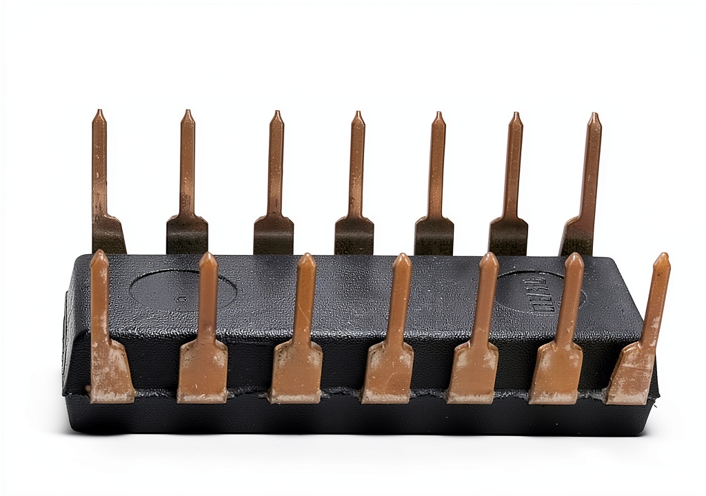
From a manufacturing perspective, the CD4027BE’s DIP‑16 package offers excellent mechanical strength and ease of handling during automated assembly processes. The lead spacing of 2.54 mm (0.1 in) aligns with common PCB design rules, reducing the risk of solder bridging and ensuring reliable solder joint formation. The package’s clear marking and robust molding compound provide visual identification and protection against moisture ingress, extending the component’s shelf life and operational lifespan in demanding environments.
Overall, the CD4027BE presents a balanced combination of speed, voltage flexibility, low power consumption, and dependable performance, making it a versatile choice for designers seeking a proven solution for digital timing, sequencing, and control functions. Whether used in hobbyist projects, academic laboratories, or commercial products, the IC delivers consistent results that meet the rigorous expectations of modern electronic design.
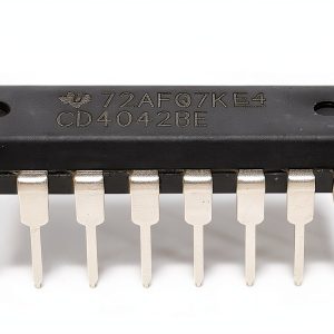
![[Product front view showing all components]](https://www.bestquickgo.store/wp-content/uploads/2026/07/f6b579af92ff4d7d826dccf5f9223dda.jpg)
Usage
The CD4027BE excels in a variety of usage scenarios where precise timing and reliable state retention are essential. In hobbyist and maker environments, the IC is frequently employed to construct binary counters, frequency dividers, and shift registers that form the backbone of custom digital displays, LED chasers, and simple microcontroller peripherals. Its ability to retain state indefinitely when the clock input is held high or low makes it ideal for creating memory elements in educational kits that demonstrate fundamental concepts of sequential logic.
In professional and industrial settings, the flip‑flop’s robust noise margins and wide supply voltage range enable its integration into control circuits for motor drives, power management systems, and communication interfaces. Designers often leverage the set‑reset feature to implement fault‑tolerant mechanisms that can quickly bring a system to a known safe state in response to external signals or internal error conditions. The IC’s moderate speed of 16 MHz is sufficient for many real‑time control loops while keeping power consumption low, an important consideration for battery‑powered or energy‑harvesting applications.
Educational institutions incorporate the CD4027BE into laboratory exercises that teach students about synchronous design, timing analysis, and the practical aspects of interfacing digital ICs with sensors and actuators. Its standard DIP‑16 footprint allows easy insertion into universal test boards, enabling rapid prototyping and hands‑on experimentation without the need for specialized tooling. The component’s compatibility with both low‑voltage (5 V) and higher‑voltage (15 V) environments provides a flexible platform for exploring the effects of supply voltage on propagation delay and power dissipation.
Why Choose Us
Choosing the CD4027BE from Texas Instruments means selecting a product backed by decades of semiconductor expertise and a global support network. TI’s commitment to quality assurance includes rigorous testing procedures that verify each device’s performance across temperature extremes, ensuring that the flip‑flop operates reliably whether deployed in a climate‑controlled laboratory or an outdoor industrial enclosure. Customers benefit from comprehensive datasheets, application notes, and reference designs that accelerate development cycles and reduce time‑to‑market.
Our distribution channels guarantee authentic, genuine parts that meet all original specifications, eliminating the risk of counterfeit components that can compromise system reliability. We provide flexible packaging options, including the convenient pack of five units, which offers cost‑effective inventory management for low‑volume production runs and educational programs. In addition, our technical support team is available to assist with schematic reviews, layout recommendations, and troubleshooting, ensuring that designers receive the guidance they need throughout the product lifecycle.
Environmental responsibility is also a priority. The CD4027BE is manufactured in facilities that adhere to RoHS compliance, limiting the use of hazardous substances and supporting sustainable design practices. By selecting this component, engineers contribute to greener electronic solutions without sacrificing performance or durability. Our commitment to continuous improvement means that future revisions will maintain backward compatibility, protecting your investment and simplifying future upgrades.
Key Features
- Fast 16 MHz toggle rate ensures responsive digital timing for a wide range of applications.
- Broad 5‑15 V supply range provides flexibility for low‑power and high‑performance designs.
- Set‑reset capability enables deterministic control of output states, simplifying circuit design.
- Low input leakage and quiescent current reduce power consumption and preserve signal integrity.
- Comes with dedicated technical support and genuine parts assurance for reliable long‑term use.
FAQ
What is the maximum operating frequency of the CD4027BE?
The device is rated for a typical toggle rate of 16 MHz when powered at 10 V, making it suitable for most medium‑speed digital applications.
Can the CD4027BE operate at a 5 V supply?
Yes, the flip‑flop supports a supply voltage as low as 5 V, allowing it to be used in low‑power circuits while still maintaining reliable operation.
What are the advantages of the set‑reset feature?
The set‑reset inputs provide a straightforward method to force the output to a known state, which is useful for initializing counters, implementing fault‑tolerant logic, and simplifying state‑machine designs.
Is the CD4027BE suitable for educational purposes?
Absolutely. Its standard DIP‑16 package, clear pinout, and robust performance make it an excellent teaching tool for demonstrating sequential logic, timing analysis, and digital circuit construction.
How does the device handle noise and voltage variations?
The IC offers full‑package noise margins of 1 V at a 5 V supply and up to 2.5 V at a 15 V supply, providing strong immunity to electrical noise and ensuring stable operation across a wide temperature range.
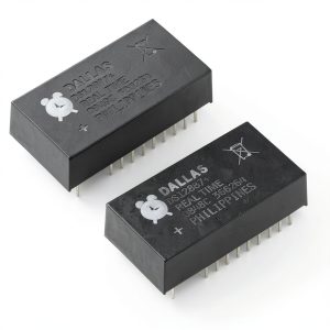 DS12887 DIP 18 Real Time Clock IC by IJJ – 2pcs Pack, Precise Timing
Reviews
There are no reviews yet.