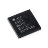

Description
Product Overview
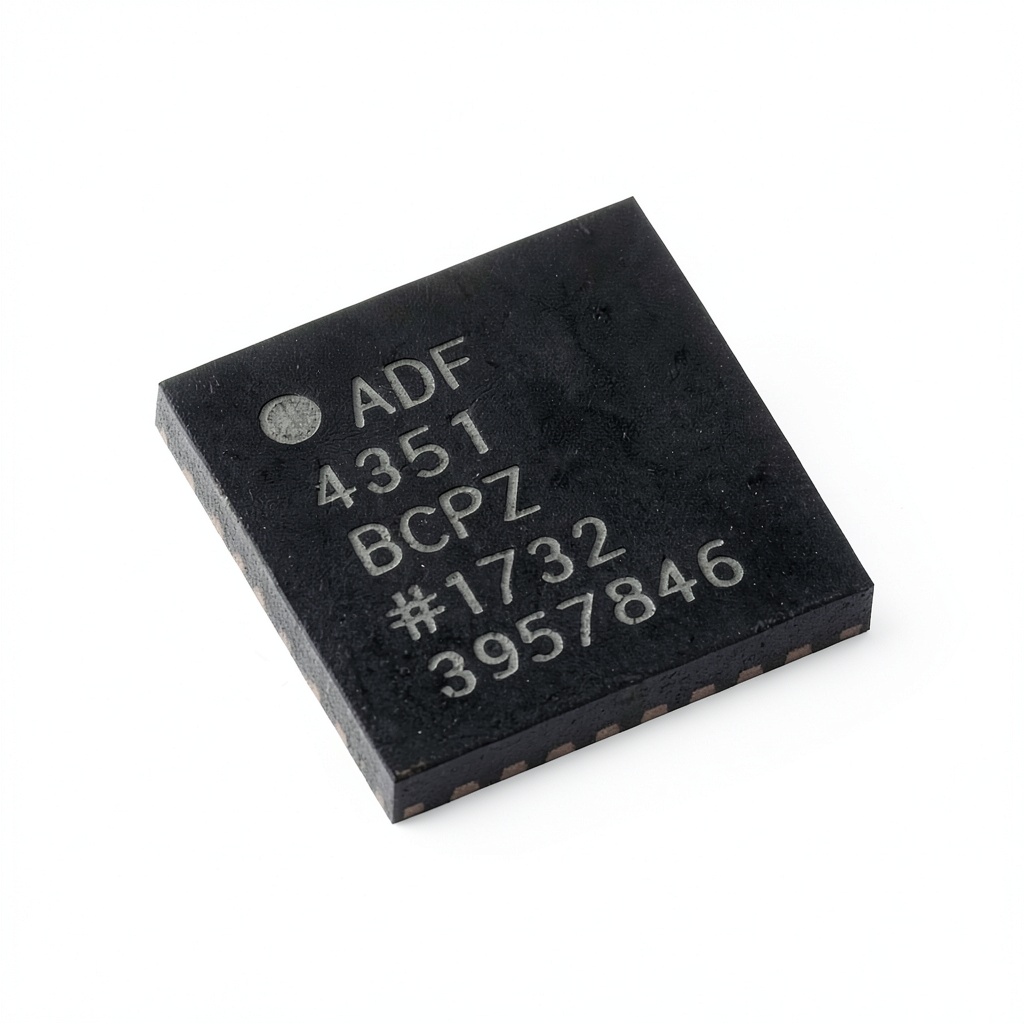
The Adf4351 Clock Generator from Nanjefly is engineered to meet the demanding requirements of modern timing and frequency synthesis applications. With a broad input frequency range of 10 MHz to 250 MHz, the device can lock onto a wide variety of reference signals, providing flexibility for designers who need to accommodate multiple standards or custom clock sources. Its internal phase‑locked loop (PLL) architecture enables output frequencies up to 4.4 GHz, delivering high‑performance clock signals for RF front‑ends, digital communication modules, and high‑speed data converters. The component is housed in a 32‑pin low‑profile flip‑chip (LFCSP) package, which offers a compact footprint of just 0.39 × 0.39 × 0.39 inches while maintaining excellent thermal performance and reliable solderability for automated surface‑mount assembly lines.
Beyond its impressive frequency capabilities, the Adf4351 integrates a suite of programmable features that simplify system design. Users can configure output division ratios, charge pump currents, and loop filter parameters through a standard SPI interface, allowing fine‑tuned control over jitter, phase noise, and lock time. The device also includes built-in reference clock doubler and divider circuits, reducing the need for external components and minimizing board space. With a typical power consumption of less than 150 mW, the generator is well suited for battery‑operated or energy‑constrained applications where efficiency is paramount.
The five‑piece lot (Adf4351bcpz 32‑Pin) ensures that engineers have sufficient inventory for prototyping, testing, and small‑scale production runs. Each unit is tested to meet stringent quality standards, guaranteeing consistent performance across the batch. The product dimensions and weight—0.39 inches per side and only 0.03 ounces—make it ideal for dense PCB layouts, especially in aerospace, automotive, and telecommunications equipment where space and weight savings translate directly into cost and performance benefits.
Manufactured by Nanjefly, a reputable supplier in the semiconductor market, the Adf4351 benefits from a robust supply chain and responsive technical support. The component’s ASIN B0DCWB2WJV and its ranking as #68 in Clock Integrated Circuits reflect its popularity among engineers seeking reliable, high‑frequency clock solutions. Whether you are developing a new wireless transceiver, a high‑speed data acquisition system, or a precision timing module for scientific instrumentation, the Adf4351 provides the versatility and performance needed to achieve your design goals.
![[Product front view showing all components]](https://www.bestquickgo.store/wp-content/uploads/2026/07/9437fe55497e4498a29941dcaafb6b2c.jpg)
Usage
In communication systems, the Adf4351 serves as a core frequency synthesizer for transceivers operating in the L‑band, S‑band, and higher frequency ranges. Its ability to generate stable, low‑jitter clock signals ensures reliable data transmission and reception, reducing error rates in both digital and analog modulation schemes. Designers of software‑defined radios (SDR) often rely on the device’s programmable output to quickly adapt to changing frequency allocations, making it a valuable asset in flexible, multi‑standard platforms.
Test and measurement equipment, such as spectrum analyzers, signal generators, and network analyzers, benefit from the Adf4351’s precise frequency stepping and fast lock times. By integrating the generator directly onto the instrument’s motherboard, manufacturers can achieve tighter synchronization between internal modules, improving measurement accuracy and repeatability. The component’s low power draw also helps extend the operational life of portable test gear, which is essential for field engineers and technicians.
In scientific instrumentation, the Adf4351 is frequently employed in timing modules for particle accelerators, laser systems, and high‑resolution data acquisition units. Its programmable division ratios allow synchronization with external triggers and reference clocks, facilitating coordinated measurements across multiple subsystems. The robust LFCSP package ensures reliable operation under varying temperature conditions, a critical factor for experiments conducted in controlled laboratory environments or harsh field settings.
Why Choose Us
Nanjefly’s commitment to quality is reflected in the rigorous testing procedures applied to every Adf4351 unit. Each chip undergoes comprehensive electrical characterization, thermal cycling, and reliability assessment before it reaches the customer, ensuring that performance specifications are consistently met. This dedication to excellence reduces the risk of field failures and minimizes downtime for end‑users, providing peace of mind for mission‑critical applications.
Our supply chain is optimized for rapid fulfillment, with inventory strategically positioned in key distribution centers worldwide. This enables engineers to receive the five‑piece lot quickly, accelerating prototype development cycles and shortening time‑to‑market for new products. In addition, Nanjefly offers detailed datasheets, application notes, and reference designs that help customers integrate the Adf4351 efficiently, reducing engineering effort and shortening the learning curve associated with high‑frequency clock generation.
Customer support is a cornerstone of our service model. Our technical support team is available to assist with design queries, firmware integration, and troubleshooting, providing personalized guidance throughout the product lifecycle. Whether you need help configuring the SPI registers, optimizing loop filter components, or interpreting performance metrics, our experts are ready to collaborate and ensure your project succeeds.
Key Features
- Broad input range of 10‑250 MHz accommodates diverse reference sources for flexible system design.
- High output capability up to 4.4 GHz delivers fast, low‑jitter clocks for demanding RF and digital applications.
- Compact 32‑pin LFCSP package saves board space while providing excellent thermal performance.
- Programmable via standard SPI interface, enabling easy configuration of division ratios, charge pump currents, and loop filter settings.
- Dedicated Nanjefly technical support and comprehensive documentation ensure smooth integration and reliable operation.
FAQ
What is the maximum output frequency the Adf4351 can generate?
The device can produce frequencies up to 4.4 GHz, making it suitable for high‑speed communication, data conversion, and RF front‑end applications that require precise clock signals.
How many pins does the LFCSP package have, and why is this important?
The LFCSP package contains 32 pins, providing enough I/O for the PLL, SPI interface, power, and ground connections while maintaining a low‑profile footprint that is ideal for dense PCB layouts.
Can the Adf4351 be used in battery‑powered devices?
Yes, the generator typically consumes less than 150 mW, which is low enough for many battery‑operated systems, especially when combined with power‑saving techniques such as disabling unused outputs.
Is there documentation available for integrating the Adf4351 into a design?
Nanjefly provides a complete datasheet, application notes, reference schematics, and evaluation board layouts that guide engineers through hardware design, firmware programming, and performance optimization.
What kind of support does Nanjefly offer after purchase?
Customers receive access to a dedicated technical support team, firmware updates, and design assistance throughout the product’s lifecycle, ensuring long‑term reliability and satisfaction.
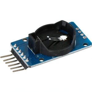
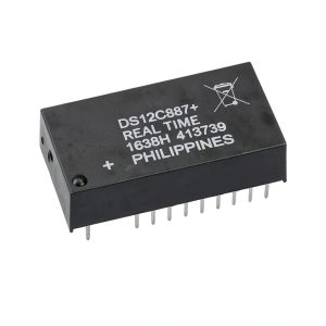 DS12887A Real Time Clock 5pcs DIP-18 New 2025 NINOMAERIA
Reviews
There are no reviews yet.